
< NoobTron TechWork |4 Months >
Executive Program in PCB Testing, ATE & Diagnostic Engineering
Built for aspiring Test Engineers and Electronics Professionals who want to develop expertise in PCB testing methodologies, automated test systems, fault diagnosis, troubleshooting techniques, functional validation, and production-level diagnostic engineering.
Specialization in PCB Diagnostics, VI Analysis, ATE Operations & Failure Analysis
Industry-Aligned. Future-Ready.





Learn industry-relevant methodologies and tools from leading organizations shaping the future of electric mobility and energy storage.
Hands-on Training. Real-world Tools. Career Ready.
DURATION
1 Month
Intensive, hands-on training with real-world projects.
FOCUS
PCB Testing, ATE & Diagnostic Engineering
PCB Diagnostics, VI Analysis, ATE Operations & Failure Analysis
LEARN
From Industry Experts
Build, test & apply diagnostics and testing solutions with confidence.
OUTCOME
Job-Ready Skills
Build, test & validate battery and BMS solutions and apply them with confidence.
NOTE:This program is focused on PCB Testing, ATE & Diagnostic Engineering.
PCB DIAGNOSTICS IS NOW INTELLIGENT
Other programs teach PCB repair.
We teach you to diagnose, validate and troubleshoot electronic systems with confidence.
Every module combines practical testing, fault diagnosis, VI analysis, ATE exposure, and real-world troubleshooting workflows. Here's how:
Industry-Aligned Curriculum
Learn PCB testing methodologies used by leading electronics manufacturers.
Hands-On Diagnostic Labs
Perform real testing, troubleshooting, and fault isolation activities.
ATE & Validation Exposure
Understand automated testing workflows used in production environments.
Real-World Fault Analysis Projects
Diagnose, analyze, and document electronic failures like a professional test engineer.










4 Unique Learning Paths that are not just lessons
From your first circuit test to advanced diagnostics, every step is hands-on, industry-relevant, and career-focused.
Learn board bring-up, power path analysis, continuity checks, signal tracing, and fault isolation techniques used by professionals.
Master VI signature analysis, component-level diagnostics, short detection, and root cause analysis with real-world failure scenarios.
Get hands-on with Automated Test Equipment, boundary scan, functional testing, and validation workflows used in electronics manufacturing.
Work on industry-like projects, document failures, suggest fixes, and build job-ready skills that make you stand out in the field.











A process built for results
Clear milestones, constant communication, and zero hand-waving. Here’s how we get from idea to impact.
STEP 1
Discovery & Success Criteria
We map your current workflows, identify bottlenecks, and define clear metrics for success.
STEP 2
Map Workflows + Data Access
We map your current workflows, identify bottlenecks, and define clear metrics for success.
STEP 3
Build + Test + Security Review
We map your current workflows, identify bottlenecks, and define clear metrics for success.
STEP 4
Launch + Monitor + Iterate
We map your current workflows, identify bottlenecks, and define clear metrics for success.
A step-by-step guide
Clear milestones, constant communication, and zero hand-waving. Here’s how we get from idea to impact.
STEP 1
Explore the Program Curriculum
PCB Testing, ATE & Diagnostic Engineering

Review the detailed curriculum, modules, tools, and learning outcomes designed for real-world PCB testing and diagnostic engineering roles.
STEP 2
Submit your application
Fill in your basic details, academic background, and work experience (if any). Upload the required documents and complete your application.
STEP 3
Registration completion
Once your application is reviewed and approved, complete the registration process by making the payment to confirm your seat in the batch.
STEP 4
NoobTron Trainee Offer Letter, be ready with the course schedule
Be ready with the course schedule
Receive your NoobTron Trainee Offer Letter and get access to the complete course schedule, batch timeline, and onboarding resources. Get ready to begin your learning journey with NoobTron!
Note: Seat allotment is on a first-come, first-served basis. Early application is recommended.
Learn. Solve. Grow.
Solve Real-World Problems as a Software Developer
Work on real industrial challenges, collaborate with experts, and build solutions that make an impact.
Real-World Projects
Work on live industry problems from 100+ companies.
Expert Mentorship
Learn and get guidance from industry experts and senior developers.
Build & Deliver Solutions
Apply your skills to design, code, and deliver impactful solutions.
Enhance Your Portfolio
Showcase real projects and strengthen your developer portfolio.
Recognized Certification
Earn a certificate that validates your skills and boosts your career.
Program Director
Lead. Empower. Deliver Impact.
WHY CHOOSE US
Our programs help learners to use AI more confidently in day-to-day work. We combine education, real examples, and guided practice so people leave with skills they can apply immediately.
Case based Classroom
Meeting-Style Discussion & Debate
Case based Classroom
Meeting-Style Discussion & Debate
Case based Classroom
Meeting-Style Discussion & Debate
Case based Classroom
Meeting-Style Discussion & Debate
THE TIMES OF INDIA
INDUSTRY NEWS
Odisha signs deal
with Intel, 3DGS
to bring substrate manufacturing tech to India
- May 29, 2026, 10:12 PM IST
- 4 min read
DOWNLOAD REPORT
View Key Highlights
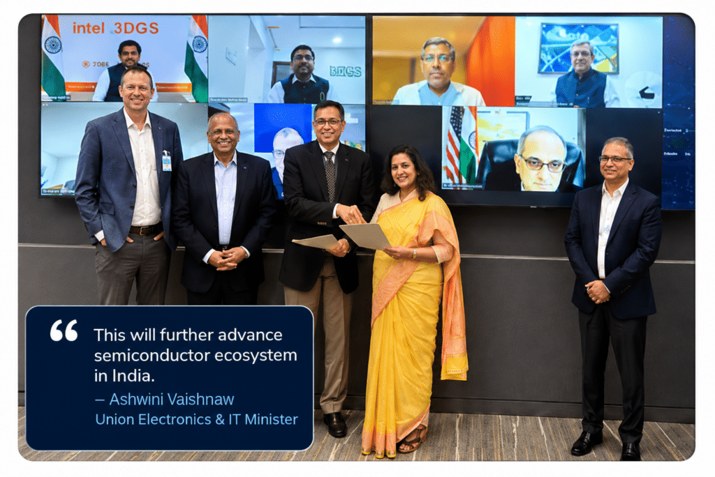
Bhubaneswar: Odisha govt on Friday signed a memorandum of understanding (MoU) with tech major Intel Corporation and 3DGS Inc USA to bring substrate manufacturing technology to India, Union electronics and IT minister Ashwini Vaishnaw said.
INVESTMENT
US$ 3.3 billion
(more than Rs 31,600 crore)
ONE OF THE LARGEST
High-technology manufacturing investments in India
EXPECTED JOBS
Over 1,800 direct high-skilled jobs to be created
TECHNOLOGY FOCUS
Advanced packaging, glass core substrates & high-density interconnect substrates
Vaishnaw, in a social media post, wrote, "This will further advance semiconductor ecosystem in India." The Union minister along with CM Mohan Charan Majhi and CEO, Intel, Lip-Bu Tan witnessed the MoU signing by officials digitally.
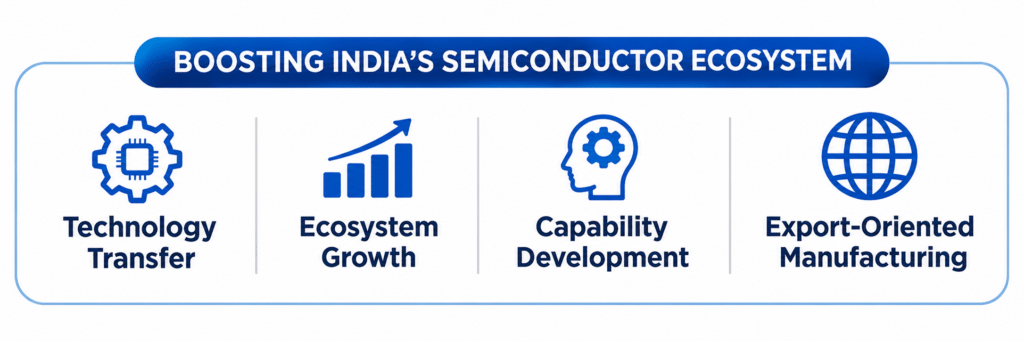
Vaishnaw said the landmark pact aligns with the Centre's vision to build a comprehensive semiconductor ecosystem. The project will be implemented in phases over 5–6 years and is expected to generate over 1,800 direct high-skilled jobs, besides significant indirect employment, the statement added.
0–2 YEARS
Engineering Graduates, Diploma Holders & Entry-Level Electronics Technicians
Engineering Graduates, Diploma Holders & Entry-Level Electronics Technicians
You understand electronics fundamentals. Now develop the practical testing and diagnostic skills used by PCB testing engineers, validation teams, and electronics manufacturing organizations.
WHAT YOU’LL GAIN
Hands-on PCB testing and troubleshooting techniques
Practical exposure to Automated Test Equipment (ATE)
VI Signature Analysis for component-level fault diagnosis
PCB fault isolation, failure analysis, and repair methodologies
2–5 YEARS
Electronics Engineers, Test Engineers & Production Engineers
Electronics Engineers, Test Engineers & Production Engineers
Advance from routine testing to systematic diagnostics and automated validation workflows used in modern electronics manufacturing environments.
WHAT YOU'LL GAIN
Advanced fault diagnosis and root-cause analysis techniques
Functional testing, boundary scan, and diagnostic workflows
Test program execution and ATE-based validation
Real-world troubleshooting strategies for complex PCB assemblies
5–10 YEARS
Senior Test Engineers, Validation Engineers & Quality Professionals
Senior Test Engineers, Validation Engineers & Quality Professionals
Strengthen your expertise in test engineering methodologies, failure analysis, and production-level diagnostic strategies.
WHAT YOU'LL GAIN
Production test optimization and fault coverage concepts
Advanced diagnostic methodologies and failure investigation
Test process improvement and quality assurance techniques
Leadership capabilities in electronics testing and validation teams
10+ YEARS
Test Managers, Technical Leads & Electronics Manufacturing Leaders
Test Managers, Technical Leads & Electronics Manufacturing Leaders
Build strategic capabilities to oversee testing operations, diagnostics programs, and reliability initiatives across complex electronics products and manufacturing environments.
WHAT YOU'LL GAIN
Advanced test strategy and diagnostic engineering frameworks
Failure analysis and corrective action planning
Manufacturing quality and reliability enhancement approaches
Leadership in PCB testing, validation, and electronics diagnostics
“I wanted more than basic troubleshooting. This program helped me understand how industry professionals perform PCB diagnostics, ATE-based testing, and failure analysis with confidence.”
Who is NoobTron ElectroLab For?
Engineering Students & Fresh Graduates
Build industry-ready skills in PCB Testing, Fault Diagnosis, VI Analysis, and Electronics Troubleshooting through hands-on practical training and real-world diagnostic workflows.
Electronics Technicians & Service Engineers
Upgrade from conventional repair practices to professional diagnostic engineering methodologies used for component-level fault isolation, validation, and failure analysis.
Test, Validation & Production Engineers
Gain practical exposure to Automated Test Equipment (ATE), Functional Testing, PCB Diagnostics, and Quality Validation processes used in modern electronics manufacturing environments.
Industry-Focused Curriculum for Advanced EV Battery Systems & BMS Engineering
Module 1
Introduction to PCBs & Basic Testing Concepts
- What is a PCB? Layers, traces, vias, pads — visual anatomy
- Why PCBs fail: manufacturing defects, solder issues, shorts, opens
- Introduction to multimeters: voltage, resistance, continuity modes
- Reading component values: resistor color codes, capacitor markings
- Safe lab practices: ESD, power handling, polarity awareness
- VCC–GND fundamentals: power rails, ground planes
- Manual short detection: step-by-step continuity testing
- PCB anatomy exercise: label all visible features on a sample board
- Multimeter drill: measure R, C, continuity on passive components
- Manual short detection: find VCC–GND shorts using continuity mode
Module 2
Passive Component Identification & Basic VI
- Passive components in depth: resistors, capacitors, inductors
- Introduction to VI (Voltage–Current) signature analysis
- What a VI curve shows: basic shape interpretation for R, C, L
- Good vs. faulty component signatures — visual recognition
- Diodes and LEDs: basic function and forward voltage
- Introduction to standalone VI testers: setup and operation
- Common measurement mistakes and how to avoid them
- Capture VI signatures of known-good R, C, L components
- Compare good vs. faulty component VI curves side-by-side
- Diode forward voltage measurement and LED polarity check
Module 3
Understanding Semiconductors & Basic Functional Tests
- Introduction to semiconductors: diode, Zener, BJT, MOSFET basics
- How to test transistors (BJT) with a multimeter
- Introduction to functional testing: what does “functional” mean?
- Go/No-Go testing concept: pass/fail criteria
- Power-on tests: what to observe (voltage levels, current draw)
- Visual inspection checklist: cold solder joints, bridges, lifted pads
- Introduction to simple test scripts (block diagram level)
- Test BJT and diode samples with multimeter; classify as good/faulty
- Perform Go/No-Go power-on test on a sample development board
- Visual inspection exercise: identify 5 planted defects on a PCB sample
Module 4
Introduction to Soldering & PCB Rework
- Soldering iron basics: tip types, temperature selection, tin and clean
- Solder types: leaded vs. lead-free, flux-core solder
- Through-hole soldering technique: heat joint, apply solder
- Common soldering defects: cold joints, bridges, insufficient solder
- Introduction to desoldering: wick and pump methods
- Introduction to SMD components and their packages
- Safety: fumes, burns, ESD, workbench setup
- Solder 10 through-hole components onto a practice PCB
- Identify and rework 3 intentionally defective solder joints
- Desolder a through-hole component using wick and pump
Module 5
Basic ATE Awareness & Lab Evaluation
- What is ATE? Overview of automated vs. manual testing
- Types of PCB testing: manufacturing, functional, silicon debugging
- Fault modeling basics: stuck-at faults, bridge faults, open faults
- Introduction to test coverage and fault sampling
- Overview of advanced tools: flying probe, boundary scan (conceptual)
- Reading a simple test report: pass/fail, fault codes
- Recap: putting it all together — diagnosis workflow
- ATE demonstration walkthrough: observe an automated test run
- Interpret a provided test report and list all detected faults
- Final evaluation: diagnose a seeded-fault board using all methods learned
Technical Pre-requisites
- Linux Basics
- Networking Fundamentals
- Basic Programming Knowledge
- Understanding of Cloud Concepts
- GCP Enterprise Infrastructure Deployment
- Kubernetes Cluster on GKE
- Cloud-native Application Deployment
- BigQuery Data Analytics Platform
- Google Compute Engine
- Google Kubernetes Engine (GKE)
- Cloud Storage & IAM
- BigQuery & Cloud Monitoring
Module 1
Track Short Detection & Advanced Strategies
- VCC–GND short detection: methods, measurement thresholds
- Traditional strategies: isolation, divide-and-conquer, injection
- Advanced strategies: thermal imaging, TDR, short-locator tools
- Short locator tool features: current injection, voltage mapping
- Fault modeling: bridge faults, resistive shorts, stuck nodes
- ATE-based short identification: setup and test execution
- Test coverage and sampling strategies explained
- Use a short locator tool to pinpoint injected short defects
- ATE-based short detection: run scan and interpret results
- Comparison study: manual vs. ATE vs. short locator efficiency
Module 2
VI Trace Analysis & QSM VI Techniques
- QSM VI: Quick Scan Mode — architecture and advantages
- Best Curve Fit Analysis: theory, tolerance matching
- VI signatures for all active devices: BJT, MOSFET, SCR, Opto-Coupler
- Semiconductor VI patterns: Zener, Schottky, in-circuit effects
- Faulty device identification: signature deviation analysis
- In-circuit vs. out-of-circuit VI measurement considerations
- Building a component signature reference library
- Capture and catalog QSM VI signatures for 10 component types
- Apply best curve fit to identify tolerance deviations
- Diagnose a board with 3 seeded faults using VI analysis only
Module 3
Functional Testing & ATE Test Programs
- Functional testing modes: OCFT and ICFT explained in depth
- Design Rule Check (DRC): what it covers and why it matters
- Analog/DAC/ADC testing using ATE: measurement windows
- Introduction to QDDL and Python scripting for test flows
- TPS (Test Program Set) development basics: structure and syntax
- TPS execution, result logging, and debugging
- ATE-based functional testing flow: board setup → test → report
- Write and execute a Python-based test script for a sample board
- Run analog/digital functional tests on ATE with real boards
- Develop a simple TPS and debug a failing test case
Module 4
Introduction to Boundary Scan Testing
- IEEE 1149.1 architecture: TAP controller, BSR, IR, DR registers
- JTAG interface: TDI, TDO, TCK, TMS pin roles
- Scan chain test: how data shifts through the boundary scan chain
- Interconnect test: detecting opens and shorts between IC pins
- Cluster test: testing non-BS logic with BS infrastructure
- BS Adapters: testing non-boundary scan devices
- Real-time fault identification via scan diagnostic output
- Set up a JTAG scan chain on a compatible development board
- Run interconnect test and trace detected faults to net names
- Test a non-BS device using a BS adapter and interpret results
Module 5
SMD Soldering, Rework & Board Evaluation
- SMD component packages: 0402, 0603, SOT-23, SOIC, QFP
- Reflow soldering: solder paste, stencil, temperature profile
- Wave soldering fundamentals: preheat, flux, wave parameters
- Hot-air rework station: nozzle selection, temperature and airflow
- Card edge testing: connector-based board-level testing
- Flying probe method: probe positioning and test sequence
- Test report generation and fault traceability
- Solder 0603 and SOT-23 SMD components by hand and rework
- Remove a SOIC IC using hot-air station without damaging pads
- Final board diagnosis: combined short, VI, and functional test
- Beginner level completed
- Comfortable with Django MTV
- Basic JavaScript knowledge
- Familiar with HTML forms
- Task manager with user accounts
- AJAX live updates (add/complete)
- User profile with photo upload
- Role-based dashboard access
- Class-Based Views mastery
- Full authentication system
- AJAX + Django integration
- Advanced ORM queries
Technical Pre-requisites
- Linux Basics
- Networking Fundamentals
- Basic Programming Knowledge
- Understanding of Cloud Concepts
- GCP Enterprise Infrastructure Deployment
- Kubernetes Cluster on GKE
- Cloud-native Application Deployment
- BigQuery Data Analytics Platform
- Google Compute Engine
- Google Kubernetes Engine (GKE)
- Cloud Storage & IAM
- BigQuery & Cloud Monitoring
Module 1
Advanced Fault Modeling & Test Strategy Design
- Advanced fault models: delay faults, crosstalk, intermittent faults
- Fault coverage metrics: ATPG concepts and fault grading
- Statistical sampling: defect-level calculations, quality goals
- Test strategy architecture: multi-stage test, ICT + functional + BST
- Cost of test vs. escape rate trade-off analysis
- Short locator advanced use: resistive shorts, partial bridges
- Thermal profiling and IR thermography as diagnostic aids
- Perform fault coverage analysis on a sample test program
- Detect and locate a resistive short using advanced locator techniques
- Design and document a multi-stage test strategy for a real board
Module 2
Deep VI Analysis & Silicon Debugging
- Silicon debugging methodology: isolate, stimulate, observe, correlate
- VI analysis of complex ICs: op-amps, regulators, bus transceivers
- Advanced best curve fit: statistical tolerance windows, Gaussian fitting
- In-circuit VI challenges: parallel path effects, loading, clamping
- ESD damage signatures and latent failure patterns in VI curves
- VI-guided component substitution strategy
- Case studies: real-world VI-based diagnosis scenarios
- VI-diagnose a board with mixed analog/digital IC failures
- Apply advanced curve fitting to identify latent ESD damage
- End-to-end silicon debugging exercise with unknown fault board
Module 3
Advanced TPS Development & VHDL/Python Automation
- VHDL-based test: stimulus generation, response capture, assertion
- Advanced Python TPS: parameterized tests, loops, fault injection
- Graphical test tools: schematic-linked test flow design
- OCFT vs. ICFT strategy: when to apply each and combined approaches
- DRC integration into TPS: automatic rule-based test gating
- TPS version control, regression testing, and CI integration
- ATE calibration, fixture design, and probe card considerations
- Develop a complete TPS for an analog+digital mixed-signal board
- Implement VHDL stimulus for a digital functional block test
- Regression test a TPS and fix three intentionally broken test cases
Module 4
Advanced Boundary Scan & DFT Implementation
- IEEE 1149.1 deep dive: BSDL files, instruction registers, opcode maps
- Scan chain diagnostics: fault diagnosis using JTAG scan data
- Cluster testing complex logic: memory, CPLDs, FPGAs via BS
- 1149.6: AC-coupled interconnect testing (high-speed SerDes)
- DFT (Design for Testability): test points, JTAG insertion guidelines
- Multi-board BST: testing across connectors and backplanes
- Integrating BST into a production test flow
- Write and load a custom BS instruction sequence using BSDL files
- Diagnose a multi-device scan chain with an injected interconnect fault
- Review a PCB layout for DFT compliance and propose improvements
Module 5
Capstone: Full-Board Diagnosis & Production Test Integration
- Production test flow design: ICT → BST → functional → final test
- Test fixture design: vacuum fixtures, bed-of-nails, pogo pins
- Failure analysis workflow: from symptom to root cause to CAPA
- Component Fault Library: building and maintaining for future reference
- BGA rework: reballing, stencil paste, controlled reflow
- Test data analytics: yield tracking, Pareto of defect types
- Documentation: test spec, traceability matrix, sign-off criteria
- Diagnose a complex board with 5 unknown faults using full test suite
- Document a complete failure analysis report with root cause
- Present and defend test strategy to peer review panel
Technical Pre-requisites
- Linux Basics
- Networking Fundamentals
- Basic Programming Knowledge
- Understanding of Cloud Concepts
- GCP Enterprise Infrastructure Deployment
- Kubernetes Cluster on GKE
- Cloud-native Application Deployment
- BigQuery Data Analytics Platform
- Google Compute Engine
- Google Kubernetes Engine (GKE)
- Cloud Storage & IAM
- BigQuery & Cloud Monitoring
NoobTron ElectroLab Alumni work at leading electronics and test engineering companies across the globe.













































Speak with a PCB Testing & Diagnostic Engineering Career Advisor
Get personalized guidance on PCB Testing, ATE Operations, Diagnostic Engineering, career opportunities, course curriculum, fees, and batch schedules.
By registering, you agree to NoobTron TechWorks’ Terms & Privacy Policy.
FEES & ENROLLMENT
Starting at ₹6,667 / Month*
Total Program Fee ₹80,000*
Master PCB Testing, ATE Operations, VI Analysis, Diagnostics, Functional Validation, and Failure Analysis through intensive hands-on training designed for aspiring Test Engineers and Electronics Professionals.
WHAT’S INCLUDED
Flexible EMI Options Available
Convenient monthly payment plans for students and working professionals.
Complete Access from Day 1
All modules, laboratory sessions, diagnostic exercises, and learning resources included.
Industry-Focused Practical Training
Hands-on exposure to PCB Testing, Troubleshooting, ATE Concepts, VI Analysis, and Failure Diagnostics.
Career Guidance & Technical Mentorship
Technical mentoring, career guidance, resume support, and interview preparation assistance.
Our Success Lies in Our Learners’ Career Transformation Stories
Read how NoobTron ElectroLab learners developed practical expertise in PCB Testing, ATE Operations, Diagnostics, and Failure Analysis through hands-on industry-focused training.
"The PCB Testing & Diagnostic Engineering program helped me bridge the gap between academic knowledge and industry expectations. The hands-on exposure to PCB troubleshooting, VI analysis, and fault isolation techniques significantly improved my confidence in handling real electronic systems. The practical approach of the training made complex concepts easy to understand and apply."
"I was looking for a specialized program focused on diagnostics and testing rather than general electronics. The exposure to ATE workflows, functional testing methodologies, and failure analysis techniques provided valuable insights into professional test engineering practices. The real-world case studies and diagnostic exercises were particularly beneficial."
"The structured curriculum and practical diagnostic sessions helped me understand how electronics manufacturers perform PCB validation and fault diagnosis. The modules on VI signature analysis, troubleshooting workflows, and root cause investigation enhanced my technical problem-solving skills considerably."
"This program provided an excellent foundation in PCB diagnostics and testing methodologies. Learning industry-standard approaches to fault isolation, failure analysis, and validation helped me gain practical knowledge that can be directly applied in manufacturing and service environments. The training was highly relevant and professionally delivered."
Ready to Become a Google Cloud Professional?
CERTIFICATE
Validate Your Expertise. Showcase Your Technical Capability.
Earn a professional certification that reflects your practical understanding of PCB Testing, Diagnostic Engineering, and Electronics Validation processes.
The NoobTron ElectroLab Certificate of Excellence is designed to demonstrate industry-relevant competencies acquired through intensive hands-on training, diagnostic exercises, and real-world testing scenarios.

WHERE PCB TESTING & DIAGNOSTIC ENGINEERING TAKES YOU
Electronics products don’t test themselves.
Every PCB, device, and electronic system requires skilled engineers to validate, diagnose, and ensure reliability.
As global investments in electric vehicles, battery manufacturing, Battery Management Systems (BMS), and energy storage continue to accelerate, organizations are actively seeking engineers with specialized battery engineering skills.
$1+ Trillion
Global electronics manufacturing industry projected to exceed USD 1 trillion in value, driving demand for testing, validation, quality, and diagnostic engineering professionals.
Source: Global Electronics Manufacturing Industry Reports
100%
Every electronic product—from consumer devices and automotive electronics to aerospace and medical systems—requires testing, validation, and quality assurance before deployment.
Industry Standard Engineering Practice
Millions
Millions of PCBs are manufactured globally every day, requiring skilled professionals for fault diagnosis, validation, troubleshooting, and production testing activities.
Global Electronics Manufacturing Ecosystem
24/7
Modern electronics manufacturing facilities operate continuous testing and quality validation processes to ensure product reliability, compliance, and performance.
Electronics Manufacturing Operations Standard
A specialized industry-oriented training program focused on PCB Testing, Diagnostics, VI Analysis, ATE Fundamentals, Functional Validation, and Failure Analysis used in modern electronics environments.
The program is suitable for Engineering Students, Fresh Graduates, Electronics Technicians, Service Engineers, Test Engineers, Production Engineers, and Electronics Professionals.
The curriculum emphasizes practical testing, diagnostics, troubleshooting, and real-world engineering workflows rather than only theoretical concepts.
You will learn PCB Testing, Fault Isolation, VI Signature Analysis, Functional Testing, Diagnostic Methodologies, Failure Analysis, and ATE-based validation concepts.
Yes. Troubleshooting, fault diagnosis, root cause analysis, and systematic fault isolation form a major part of the training.
Yes. The curriculum is designed around testing and validation practices commonly used in electronics manufacturing and service industries.
Yes. Learners perform practical diagnostic exercises, testing procedures, troubleshooting activities, and fault analysis sessions.
Training includes exposure to Multimeters, Oscilloscopes, VI Analysis concepts, PCB Diagnostic Tools, Functional Testing Platforms, and ATE workflows.
Yes. Multiple diagnostic exercises and fault-analysis case studies are incorporated to simulate real-world electronics testing environments.
Yes. Participants who successfully complete the program will receive the NoobTron ElectroLab Certificate of Excellence.
Absolutely. The certification demonstrates your practical competency in PCB Testing, Diagnostics, Validation, and Failure Analysis.
Yes. Learners receive career mentoring, technical guidance, and support for preparing professional profiles and interviews.
Potential roles include PCB Test Engineer, Electronics Test Engineer, Validation Engineer, Diagnostic Engineer, Quality Engineer, Manufacturing Engineer, and Service Engineer.
Consumer Electronics, Automotive Electronics, Aerospace, Defence Electronics, Medical Devices, Semiconductor Manufacturing, Industrial Automation, and Electronics Manufacturing Services (EMS).
Yes. Every electronic product requires testing, validation, diagnostics, and quality assurance before deployment.
Yes. Flexible EMI plans are available for eligible participants.
The fee covers training sessions, learning materials, practical exercises, diagnostic workshops, assessments, and certification.
You can complete the registration process through the admissions team and confirm your enrollment by completing the fee payment process.
#Transform with Purpose